|
|
|
|
PCB FAQ Version 3.0
Use of information in this faq is solely at the users risk. No liability will be accepted for any damage or loss resulting from the use or abuse of information contained in this document.
Read the disclaimer below attentively before building or using any of the described equipment and procedures. Vincent September 5th 2000.
THE AUTHOR OF THIS FAQ , CANNOT BE HELD RESPONSIBLE FOR ANY DAMAGE OR INJURY TO ANYONE OR ANYTHING RESULTING FROM THE USE OF WHAT IS DESCRIBED IN THIS FAQ. SOME OF THE THINGS EXPLAINED IN THIS FAQ HOLD A POTENTIAL DANGER OF ELECTROCUTION OR POISONING OR INJURY WHEN BUILDING OR USING THEM. YOU ,THE READER OF THIS FAQ, AND ONLY YOU ARE THE SOLE PERSON RESPONSIBLE FOR WHATEVER MIGHT HAPPEN. WHEN YOU BUILD ANYTHING FROM THIS FAQ AND SELL IT ,RENT IT OR GIVE IT TO THIRD PARTY PERSONS, YOU ARE RESPONSIBLE , AND SHOULD TAKE PRECAUTIONS TO INFORM THE USER ABOUT THE CORRECT PROCEDURES. WHEN USING THE CHEMICALS DESCRIBED IN THIS FAQ YOU MUST TAKE ALL NECESSARY PRECAUTIONS TO PROTECT ANYONE OR ANYTHING ELSE FROM INJURY OR DAMAGE RESULTING FROM THE USE OF THESE PRODUCTS. IN DISPOSING OF USED CHEMICALS YOU MUST FOLLOW LOCAL REGULATIONS. PLEASE TAKE CARE OF MOTHER EARTH !.
Before you can start making a Printed circuit board you
need a layout. If you already have on (from a magazine or so) you can skip this section.
and go to the next section. What will be discussed here are the techniques and materials
involved in the drawing process and the drawing methods. This section focuses mainly on
the photo graphical process of making a PCB. If you are going to make a unique and simple
board you might consider to draw directly on copper clad material. This is discussed in
the next section as well.
Making a PCB Layout for Photographic PCB production.
Using pen and paper
You can also make your drawings on tracing paper. This is a
semitransparent type of paper. This is good solution if you make your PCB by photographic
means. There also exist transfer symbols that make life easier. Check out your electronics
store.
Most of these programs are intended for professional use and cost a lot of money. However a number of those programs exist in a time limited version or in a so called 'student' version. Mostly the number of pins and / or board size is limited and you cannot create Gerber files ( more later ). Software makers often have evaluation versions available for download. check the last section of this FAQ for some web links. So far for the software. Let's see what is needed more. In the
end what counts is that you get your design on paper or drafting film.
A Laser printer uses a 'toner' (the black powder used to print). This toner will cause big filled area's to appear 'shaded'. The application of the powder is not even throughout the printed field. Since an ink jet printer is using liquid ink this is not the case. The printout will be equally black on all places. Furthermore a laser printer has the so called 'warping' effect. The drum of a laser printer is never perfectly round. This will result in the local compression and expansion of area's. This might render a layout unusable. The last problem is that the printer melts the toner into the transparency. The transparency will deform and stretch. This can cause intolerable errors in the board layout. One important thing when making printouts is the quality of the paper. In Ink jet printers you should use glossy paper. The ink stays on top of the paper and does not penetrate into it. This prevents the ink from smearing out. Of course the drying process will take some more time. You can use tracing paper in all of these printers. This will save you the step of making a transparent layout further on. You can also use so called 'overhead projection transparency's'.
However , make sure that you have the right type of film for your ink jet printer. My
experience shows that the best result is obtained with HP or 3M transparencies. Using HP
transparencies and a 600 DPI ink jet printer i have made boards with traces of 6 mils. And
that is extremely fine. Most professional PCB makers will already charge you extra to make
that kind of board.
The main drawback is that plots are costly. Not only the plotter itself is expensive but the cost involved in making a plot is substantial too. The pens and the special paper cost quite some money. this get even worse if you plot on slides. On a plotter you can also use tracing paper or transparencies.
When using these you might have to buy special pens. Check this out with the supplier of
your plotting equipment.
The plot is done in a darkroom on a photograpical film. When the plot is completed they develop it just like a regular photo. The advantage of a photo plotter is that it can plot at incredible densities. 6000 dpi is considered 'low resolution' with these machines. there are photo plotters with resolutions of over 40000 DPI. these are used for so called 'Mask Scribing' in IC design. There they plot on a chrome plated quartz disk. After photo plot the disk is etched using Plasma etching ( dry etching using a corrosive gas that is 'excited' under a strong electro-magnetic field ). This negative is then used as master to make integrated circuits. Some of these masks hold geometry's below 1 Micron . That is one thousandth of a millimetre or one 25000 Th. of an inch !.
A number of companies offer a photo plot service. Most of the PCB board manufacturers have these machines on their premises. Often you can ask them to do this. They require you to generate GERBER or DPF format files. GERBER is a standard plotting language for Photo plotters. All good PCB CAD software can generate Gerber and most of them can also generate DPF files, although not every Photo plotter can read DPF. For a home-made board this is of course overkill. If you find yourself in the need of a photo plot you can also contact offset printing businesses. They often have the capability to 'plot' postscript files to a machine similar to a photo plotter.
Chapter 2 : Transferring the layout
Now that you have a layout ready you need to get it onto copper clad material. There are three different processes : The direct draw , the transfer and the photographic process. The photographic processes all required so called 'Art-Work'.
This is the final layout on a suitable material that is going to be used for photographic
reproduction of your layout.
Drawing directly onto the PCB
material. In Europe there exists a company called Decon-Dalo. This company makes a special pen with a pumping mechanism. The ink in this pen is specially designed for etching PCB's. Its resistance against the etchant is very high. In the USA the best is to go to your local Radio Shack or check out the mail-order shops like DigiKey, Arrow, Mouser, or Newark .They have it in their catalogues. Anyhow the best to acquire a drawing pen of this type is to go to your local electronics shop and buy one there. They can also be found in print-shops. Even Staples might sell them! Furthermore you need some Clean PCB material. There are a number of different materials available. (see further on). Make sure the Copper is clean before you start drawing on it. To clean it you can use regular Scotch-Brite from 3M. Don't use steel wool. It will make the copper oxidize and generally it leaves some grease on the copper. To make it really perfect you can wipe it off with a cloth wetted with IPA. (IsoPropyl Alcohol) Now you can draw the tracks on the Copper surface. When finished make sure it gets the necessary time to dry thoroughly. When drawing prevent, as much as possible, from touching the copper with your bare hands. The grease on our skin will oxidize the copper and might make the exposed areas more resistant against etching. There are a number of companies that sell so called Dry
Transfers. These are sheets of plastic that have all sorts of symbols on them. You can
transfer them by simply rubbing on the paper. Put the sheet with symbols on the Copper.
Rub with a pencil on the symbol you want to transfer. It will stick to the copper. Sheets
exist with all sizes of Pads, Tracks, symbols. You can find addresses at the end of this
FAQ.
Using transfer films
Now you have to put the film, with the printed side, onto the bare copper. Put a regular household iron on the film. The temperature setting should be intermediate. Some experimenting might be necessary to get good results. What happens is that the printout will be transferred onto the PCB. Just let it cool down and then remove the plastic film. If you're successful you should have a neat PCB ready to etch. The film can only be used once since the process depends on the special coating of the film. What happens is that during the copying process the toner melts and reacts with the special coating on the transparency. It forms a rubbery sticky film. If you iron it on a board the temperature is lower. The sticky stuff will glue itself on the copper ( which is easier to adhere to then the mylar which composes the slide). After etching you will need to remove the layout using steel wool. Regular solvents
don't work that good. There are a number of these films around. You
can find more information at the end of this FAQ.
Using a copier and
overhead transparencies Make sure that you have transparencies designed for copiers. They
will have to stand the heat used inside the copier to make the toner stick to the carrier.
( toner = the black powder )
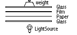
Using a contact
positive Film You need :
procedure : Put you drawing on the glass plate. Beneath the glass plate you
put the light source. Put the film on your drawing. put the second glass plate on the
film. Note: you can use something else for the top plate too. It is just used to push the
film onto the drawing. For larger drawings you should use a frosted glass plate. That
way the light is being diffused. This will give you better results. Even better is a sheet
of white Plexiglas. This is a white sheet of plastic that is transparent for light.
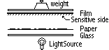
Using a contact negative photo film A more professional way is using real photofilm. This kind of film is produced, amongst others, by KODAK and AGFA. The type is LITEX no 0911p.It is the kind of film used by newspaper publishers to make their lead plates for printing newspapers. For this film a darkroom is necessary. It must be processed in RED light because it is extremely sensible to other light. You can check your local photo shop. They should be capable of giving you advice on what you need and how to do it. The cost of getting started is reasonable. You will need to purchase a box of films (sold per 100 pieces) and some chemical products. It requires some experience too before you get working results. But the result is excellent and the cost per film is very low. (around a dollar for standard letter size paper.). Black is really black on this kind of film. Basically what you need is :
Let's start at the bottom. A Darkroom. so: 1 part of Fixer for 4 parts of Water. This will give you the
right solution for the Litex Film. You will have to follow instructions on the package to make the final product. For the liquid product for instance :
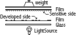
This will give you a clear solution if it's okay. It may take up to 1 minute before it comes completely clear. In the means time the colour can change between a milky solution and brown. You can hold this solution for about 1 month if you store it in a dark cold place and depending on the usage. Eventually it will go bad. Even if you don't use it. That is the reason why it is delivered as two different products. When separated they can be preserved for a long time. (Mine are currently over 5 years old). Store them in a airtight bottles in a dark place. Best is to buy special photo bottles. These are black plastic bottles that you can squeeze. They look like a harmonica. Also make sure that the product is kept cool. Around 16° Celsius Maximum. This product is rather inexpensive .The products you need to make about 5 litres of developer will cost something like 12 Dollar. The LITEX Film. The type is LITEX 0911p from AGFA. You can buy these in ready cut sheets. There are 3 or 4 different sizes which are sold in boxes of 100 films. A box of oversized Letter paper films will cost something like 100 US Dollar. You must store these films in a dry, clean, fresh and preferably dark place. Temperature must not rise above 25 degrees CELCIUS. When you respect this you can hold these films a very long time. Up to 5 years is perfectly possible. Okay. Now how is it done ?. Make sure you have made the solutions of the products you need. Also get everything else necessary. Gloves, the artwork , light unit , a pair of scissors (to cut film to size) , the box of films ,the trays, the tweezers etc. ,maybe a set of safety goggles to protect your eyes from the chemicals. Switch to DARKROOM mode. When in the red light take some time so your eyes can get used to their new environment. After a minute or so you will be amazed of what you are capable of seeing. Fill one tray with about 1 litre of mixed developer. Another with about 1 litre of Fixer. The third tray gets filled with fresh water. Open up the box of films and take out one. Cut it to the right size and store the rest back into the box. CLOSE THE BOX AGAIN !. This will prevent from exposing all of the films by accident. You will see that the films are packaged in a black plastic bag inside of the box. You will also remark the the inside of the box has been made completely black. This is done to protect the films as much as possible from ambient light. When cutting sheets of films you must cut 2 pieces. The film is of the reversing kind. You will first make a negative before making a positive again. Put your drawing with the inked side up onto the glass plate of the exposure unit. Put the film on top of the drawing. If you look at a sheet of film you will remark that it has a darker and a lighter side. Put it with the lighter side on the inked side of the drawing. The lighter side of the film is actually the sensible layer. Close the lid of the exposure unit and switch on and off. The exposure needs only a flash of light. The actual time needed for the exposure is half a second. It is sufficient that the UV lamps just flashed once or twice. Put the exposed film into the tray with the developer. Put it in with the light side UP. Be careful not to scratch the light side of the film. It is rather fragile when wet. Depending on the age of the developer and the exposure time the film will have to stay in there for 0.5 to 2 minutes. You will see that the exposed parts will turn black. The film is ready when it is equally black. Also look at the white areas. When they start to go brown the film has been in the developer too long or you have exposed it too long. The above part may take some experience. Don't get worried when the first 10 trials fail. Once you get it right you will have very rare failures. When it's okay take it out of the developer , using tweezers, or if you are wearing gloves you can do it by hand. Put the film immediately into the FIXER without rinsing !.It will have to remain in the fixer for about 2 minutes. You will see that the white area's will become transparent. There is no risk of ''over fixing'' the film. Of course if you leave it in there for over 30 minutes it will go bad. But you can safely leave it in the fixer for up to 5 minutes When it's fixed put the film into the water and leave it in there for some time (2 to 3 minutes). Then you can take it out and rinse it under running water. Be careful not to scratch it. It is very fragile when it comes out of the processing. Once it's dried up it's very tough and can stand strong abuse. Making a positive image again: This is the same as step 5 but instead of starting from the paper drawing ,start from the film you just made. What i generally do is take the film out of the tray with water , wipe it of a little and start from this wet film. What will happen is that a small layer of water will be between the the two films. This will give some optical effect and insure a good sharp result. The best way to wipe of the the film is to pull it between 2 fingers. Be careful not to cut yourself though. The edge of the film is rather sharp. There exist also special rollers to do this. Check with your photo shop. Clean up. Put all liquids back in their respective bottles and wrap up. When it's okay you should have a razor sharp image of your drawing by now. Note: The products are light sensitive too! Therefore you have to store them in black bottles. Put the liquids only into the trays when you are already in your darkroom. I have been making films with this method for the last 8 years now and so far only very few have failed. (i'm making 3 to 5 film's a week !). I can make a ready-to-run film from paper in less then 5 minutes. It is a very good way to make your PCB layout , but as i said : it takes some experience and some patience to get started. I Screwed up a number of times before i got the results i wanted. I have tested the possibilities of the Film. It is possible to make tracks of 5 mils and less !. (Starting from a Plotted artwork on a raster plotter from Versatec.) If you have layouts with tracks smaller than 15 mils then you can follow these guidelines : Print or plot the MIRRORED view. This is the view you would get if you would look trough the PCB. In the first step this will happen :
Now that we have created a layout and converted it into ARTWORK
we should start thinking about the kind of material we are going to transfer it to.
More advanced materials consist of fiber based materials or PTFE ( teflon (tm) ) . In the industry many other so called 'substrates' are used as well. A name that appears frequently is 'Rogers'. these are high quality materials used for RF boards as found in cell phones. You can buy pre cut sheets of this material either double or single sided. Several companies also make material which is pre coated with the photosensitive layer. You can also opt to make this yourself. Some chemistry companies
sell this photo-laquer in spray cans. However the end result will never be as good as the
ready made material. Moreover the process is rather messy en unhealthy. However if you really want to do it :
You must clean the Copper layer of the PCB and wipe it
off with IPA (Iso-Propyl alcohol, sometimes referred to as household or rubbing alcohol ).
When it is dried up you can spray the photo lacquer onto the copper area. You have to do
this in a darkroom ( by red light ). Make sure it gets evenly spread onto the whole copper
area. Now you must leave it to dry , in a dark place for 24 hours. You can also put it in
a oven at a low temperature ( approx. 70° centigrade ). If the layer does not stick
anymore it is ready.
Basically there are two different types available. Positive and negative. About 95 percent of the material being sold is positive material. Which is okay for what we need. The negative material is used in industrial PCB production. The only advantage is that it easier to make Multilayer PCB's with. But since this is virtually impossible to do at home : forget about it. You can recognize the material by
looking at the lacquer. Peel of a small corner of the cover sheet and look at the
photosensitive layer. If it has a light blue metal shiny look then it is negative
material. All other colours are positive material.( this is to my knowledge ).
Okay . Up till now we have been busy transferring our
drawing onto a transparent material. So now we are ready to transfer our image onto the
Copper layer of the PCB.
Exposing the PCB to the artwork For starters we need photosensitive PCB material. There are 2 possibilities here : Either you buy ready made material or you make it yourself. The best is to buy ready made material. This is a PC board of which the copper layer is covered with photosensitive lacquer. The lacquer discovered with a black paper or plastic which can easily be removed. Right. So by now we should have our artwork on a transparent medium ,the PCB and PCB developer. What else do we need : 2 plastic trays. A pair of rubber gloves and an exposure unit. This has to be an Ultraviolet light source designed to expose PCB material. The wavelength is rather important. The how-to section in this FAQ describes how you can make your
own. If you don't want to spend money you can use direct sunlight too !.
Put the film on the sensitive side of the PCB. (of course you first have to remove the cover paper). Cover it with a piece of Plexiglas or other clear plastic. Don't use glass here because it stops too much of the ultraviolet component in the sunlight. Exposure time : somewhere around 10 to 15 minutes. You should
experiment
Exposing using a dedicated exposure unit The exposure time (with the described exposure unit or with a ready made unit) is approx. 2 to 3 minutes. Some experimenting might be necessary here although it is not very critical. Put the drawing onto the exposure unit. Put the PCB with the sensible area onto the drawing , close the lid and start the exposure. Two important notes here :First : Protect yourself ! Ultraviolet light is dangerous. Never look into the light source when it is switched on. Always close the lid of the exposure unit when the lamps are turned on Second: Do this in dimmed light. Not in clear daylight. Although the PCB material is only sensible to UV light there is a risk of destroying it with direct sunlight or strong daylight. Sunlight contain UV also and strong daylight will gradually reduce the sharpness of the image. You can process PCB's in normal ambient light if you use the PCB material directly. Once the cover paper has been taken away from the photosensitive layer you must use it. Don't leave it on your table for 2 minutes. It will go bad if you do. I generally do it in ambient light. I put my transparent on the exposure unit . Take the paper away from the PCB . Put the PCB on the drawing and close the lid. After the exposure i take out the PCB and put it directly into the developer. Works all the time.
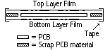
Double sided PCB's
Align the films and tape them to the PCB material. This way you get an arrangement where you can slip the PCB material between. The alignment will be ok. If you would not use the 2 strips of PCB material the risk exists that the images are shifting and the PCB becomes unusable. You need a double sided exposure unit. However if you don't have this you can just flip it over. Only thing is that you have to make sure that the PCB does not shift. Some household tape (scotch tape) will do just fine. Now you can expose , develop and etch as any normal board.
Before we can develop the exposed material we need a suitable developer solution. Generally the shop that sells the PCB material will sell also this material. There are a number of different products on the market but basically they all contain SodiumHydroxid. SodiumHydroxid is the substance used to de-clog your drain. If the drain of the kitchen sink is clogged then you can buy bottles of brown liquid to throw in there and de-clog the drain. Well the product in those bottles is most of the time SodiumHydroxid. I have tested it and it actually works to develop PCB's with. ! Of course you have to dilute it . It is far to concentrated to use directly. It is best to buy the product in an electronics shop. You will have the clean pure stuff. You can buy ready made doses of product to make 1 litre of product. Mostly it comes as pellets or in powdery form ( sort of granular looking ) When handling the product please wear gloves and safety goggles. It will probably not cause any burns but it is not very healthy to put you bare hands into the product or solution. Should you come in contact with it rinse with water. If you get it into your eyes then rinse with plenty of water and call a physician. The product destroys the natural oily protective layer on your skin. A typical solution is good for lots of boardmaking. Only point to take care of is to stored it in a closed bottle with as little air as possible. The Sodium Hydroxide goes bad upon prolonged exposure to air. It combines with he Oxygen and goes bad. So store it in a photo bottle ( a compressible plastic bottle ) MARK THE CONTENT OF THE BOTTLE CLEARLY ! So nobody uses it
abusively.
Developing the exposed material After exposing the PCB you must develop it. Therefore you have to put it into the developer. The actual developing process takes somewhere between 30 seconds and a minute. You have to move the PCB in the liquid. After some seconds you will be able to see the image on the PCB. After half a minute you should have areas with blank copper and areas that are covered with the photo resist. The photo resist will turn brown to black so you can see it very clearly. Now you can take out he PCB and rinse with water. Make sure to rinse off the board thoroughly . The product reacts with most etchants and makes them go bad. That's it. Now you have a PCB that is ready to be etched.
By now we should have a sheet of 'copper clad' material with lacquer in the pattern of the copper tracks we want. depending on your choice this could be ink based , transfer , or photo resist. The time has now come to remove the bare copper. We can be brief about the procedure here. Just put it into the etchant and wait until all bare copper has been removed. Then take it out and rinse with water. However there are lots of chemicals you can use to etch a PCB. In general when using these chemicals please wear safety goggles and gloves. Best is also to wear an acid-resitant apron. Most of
these products are capable of eating holes in your clothes or producing stains that are
very hard to remove.
While there are special mixtures known , basically
there are 2 basic products used to etch PCB's with.
There are people that mix FE3CL with other chemical products to improve the etch rate. But in general this results in the release of toxic gases. There are also some other products that can be used. Since the risk involved with these other products is bigger i will not cover them here. The products described above are ,although still dangerous, safer than others. I use Sodium or Ammonium persulfate. Mostly sodium persulfate. Ammonium persulfate is used to etch large quantities of PCB's at the same time. The problem with the product is that it tends to recrystallize if you let it cool down. Once you make a solution you must use it. If it cools down it goes bad. Sodium Persulfate solution can be stored ready made for a long time. That's about it. After etching the PCB remember to rinse it thoroughly with water.
Now you have a PCB ready to drill holes in and put components on.
Removing the resist layer
Removing the resist is best done by using IPA (
iso-propyl or rubbing alcohol ) or Acetone. If you are going to use acetone ,please do so
in a well ventilated area and wear gloves. Acetone is not so healthy for your skin.
Making trough hole connections The big question. How do you connect the 2 sides of the PCB together. There are a number of ways to do this. Use pieces of wire to put in the holes. Or recycle the cut of component leads from your previous board .A really neat way is to use a special component for this. It is called a Track Pin. It is sold as strips which you can easily break apart. The above techniques have the disadvantage that you cannot put a component in the hole anymore. When making the PCB layout you should try to make VIA's
(connections from one side to another) at the component pins directly. That way if you
solder the lead at both sides then you have an instant trough hole connection. If you use
IC sockets with machined contacts ( the round pins with the tulip sprig inside )
then you can even apply this technique for IC pins
First the holes are being drilled by a computer controlled drilling machine. The PCB now goes in a chemical plating agent. This is a special liquid which contains lots of copper in an ionic form. By running a current trough the solution and your board the ionic copper precipitates on the PCB. Both on the copper and on the bare PCB material. This way a copper layer of about 10 to 15 micron is being grown onto the PCB material. Now a NEGATIVE photo lacquer is applied and exposed with the layout. After development the tracks are bare copper ( this is exactly opposite as the process we use at home ). What has to be removed is still covered with lacquer. No i'm not mistaken here !. Read on it will come clear why. The problem with photo lacquer is that it will not penetrate into the small holes to cover them from the etchant. So they use a different technique. The PCB is now plated with TIN or Chrome. Next the photo lacquer is stripped off. You end up with a PCB where the tracks are marked with TIN or Chrome. The plating solution is able of penetrating into the holes and covering the inside wall of the whole with TIN or Chrome. To etch the PCB they use heated Sodium Persulfate. Nice thing about this is that it only etches copper. It does not etch TIN or Chrome. So the coated locations are not being etched. When the PCB is etched they clean it up and have a trough plated and tinned PCB. The chrome is used if they make multilayers. They stack
the boards on top of each other and make the chrome fuse together. Since the melting point
of chrome is higher than the one of TIN this will make sure that the board does not fall
apart if you solder it. Of course they start with thinner material to make multilayers.
The copper thickness is also much less.
Applying a solder
lacquer
Tinning boards Hot tinning can be done using a special brush like tip on a normal soldering iron. ( available from Weller or Cooper tools ) You have to make sure the board is clean ( strip off all resist
and clean thoroughly using IPA ). Then apply a soldering flux for the electronics
industry. ( Not the kind the plumber uses. That contains acids ). Simply let a generous
bit of tin melt into the brush tip. Then pull it at a constant speed over the copper
tracks. They will be nicely coated with tin. Afterward wipe off any excess flux. The plating process is very fast but it requires some precautions. The copper must be very clean. Furthermore you must prevent ,as much as possible, that strange products get into the liquid. The liquid is very sensible to other chemicals and even to water. It will go bad. The best procedure is as follows:
If you put water on a pcb that comes out of the IPA you will see that it will not stick to the copper. It will run off immediately. The PCB will look 'greasy'. However it is not. Anyhow ,for the plating process this is not good. Now wipe dry again with clean cloth or kitchen paper. Put the PCB in the plating solution and leave it in there for a
couple of minutes (1 or 2 should be sufficient) Take it out an rinse with water. Wipe it
dry immediately !. This is necessary since it will oxidize very rapidly if you don't do
this. Now you still can apply a solder lacquer if you'd like.
Silk screening the PCB
But you can use the iron-on type of films. The procedure of transferring paper to film and paper to board has been described in the section about making PCB's by hand. Simply put it on the non copper side of the board now. Another possibility is to copy on a transparency and simply stick
that to the board.
Well what could possibly be said about drilling holes in PCB material ? More than you would expect at first sight. PCB material is a rather tough stuff to drill holes in. While softer than metal it has a bad thermal conductivity. This means that your drill will heat up more faster and thus will go bad very rapidly. You can use standard HSS drills , but will notice that they loose their sharpness after approx. 50 holes. This can be seen by the fact that the copper around the hole seems to be 'pushed-up'. Time to change the drill if you see this. Another option is to use so called tungsten drills. These are a lot more expensive but are used by the PCB industry. They stay sharp for thousands of holes. But ... they have a drawback. They are made of such a hard material that they easily break . If you are going to use such drills you must make sure that the
drill does not vibrate. Furthermore they are designed to be run at very high speed (
10.000 to 30.000 RPM ).
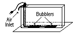
The two typical units you need can be built by yourself.
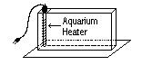
This chapter will describe how to make your own super deluxe etching unit with air pump and temperature controlled heater DISCLAIMER : I cannot and will not be held responsible for injury, damage or whatever ,either to you, third party or whatever , resulting from building or using this unit. Just to make this clear. If you decide to build and/or use this unit you are the only one responsible for whatever might happen.
a scrap piece of plexiglas or Acryl material approx. 10 by 10 cm ( 4 inch by 4 inch ) NO
GLASS FOR THIS ONE ! If you use Plexiglas (Acryl) plates then they should be at least 5 mm
(1/4 inch ) thick | Silicone glue ( the kind used in bathrooms or for securing windows in
their frame) , or an acrylic glue if you use the Plexiglas | Fine sanding paper ( one sheet medium and on sheet of the finest you can
get | Polishing cream and a soft cloth. ( not car or shoe polish ! The stuff they use to make
glasswork shine .) | Strong working gloves ( in case you use glass get some kevlar enforced gloves) | Some pieces of plywood ( an empty milk carton or milk brick will do the trick too ) | Holding clamps ( the kind carpenters use ) | Alcohol ( IPA or rubbing alcohol ) | Note : Do not cut the glass yourself unless you are skilled in this . Glass is a dangerous material. It can produce razor sharp edges and you can easily cut yourself very badly. You can obtain glass plates from a hardware store , or do it- yourself store. They should be able to cut it for you. Sometimes people specialized in aquariums can help you too. Acryl or Plexiglas is easier to obtain and can more easily be processed yourself: Preparation of the
materials Clean the plates using the alcohol. This is to remove any grease that may be left on them. Make sure that after cleaning no fingerprints are left. The grease in your fingerprints will prevent a perfect gluing of the materials. This will make the box leaky . And that's exactly what we DON'T want.. Assembling the main
structure In this piece drill a hole just big enough so you can put the heater trough. Also drill
a hole to put the air tubing. Last you connect up the small air pump to the air inlet. When using this unit make sure it is connected to mains using a Ground Fault
Interrupter . Never let this unit work unattended ! And keep other people away from it (
especially children ). After all: the stuff you will put in there is potentially
dangerous.
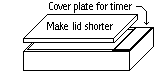
Building your own exposure unit
Of course you can buy these ready made in large electronics shops. But what is more fun than building one yourself .. and save a lot in the process too. This section will provide you with the details on how to make this sort of equipment. DISCLAIMER : I cannot and will not be held responsible for injury, damage or whatever ,either to you, third party or whatever , resulting from building or using this unit. Just to make this clear. If you decide to build and/or use this unit you are the only one responsible for whatever might happen. Basically the unit is an enclosure with a lid and a light source. Optionally you can install a timer. Depending on you skills you can build this in wood , metal or plastic. I built mine in wood. Make an enclosure (in wood ) of which the top cover is attached by hinges. So you can open it. You can ask a carpenter to help you here. The easiest way is first to make a completely closed box. The lid should be made just high so that you can put a piece of foam rubber or 'mousse' in there. You should have to apply a light pressure to be able to close it. This is to insure that the PCB and/or film makes good contact with each other when they are between the foam rubber ad the glass plate. In the back of the exposure chamber you should drill some holes so that fresh air can get into the chamber. Normally VF lamps do not produce much heat. But to improve fire safety just do it. Make the enclosure so that you can fit 4 Ultraviolet lamps inside.
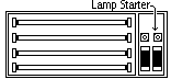
Make the exposure chamber so that the lamps are spaced about 2 inches apart and 1 inch from the walls. The best is to go to an electronics shop and buy a PCB exposure kit there. Usually they can sell you a small kit containing 2 lamps the starter, the coil and the necessary sockets. This kit will also have an electrical wiring diagram. I Cannot give the actual sizes of the box because i don't know what size of lamps you will use .You will have to make your box depending on the size of lamps you use. However: the glass plate should be approx. 4 inches away from the Lamps. The top glass plate is made from frosted or clear glass. Make sure you
have good quality glass here. It should be about = 1/4 inch thick. Cover the bottom of the exposure chamber (on the inside of course)
Keep the edges of the aluminium foil about 1 inch away from the lamp
sockets. The Aluminium foil is used as a reflector for the light that the When wiring the whole system use good quality electrical power wire and
respect all electrical cabling rules .That's about it. When you put some time and work
into it you will end up with a unit that will serve you for many years.
General material sources Digikey has a good section on PCB material in their catalogue. They even sell the VF
tubes and starter kits. they also have most of the stuff described in this FAQ.
ISO-PROPANOL MSDS Number: P6401 ACETONE MSDS Number: A0446 SODIUM HYDROXIDE MSDS Number: S4034 Sodium Persulfate MSDS Number: S4730 AMMONIUM PERSULFATE MSDS Number: A6096 Ferrous Chloride, 4-Hydrate MSDS Number: F1678
This FAQ compiles for a last time all i know about making PCB's. Will there be future updates ? I Don't know, maybe someone will take over. Currently I am stopping all my activities to do something completely different: become a dive instructor and go and live on a little island in the indian ocean far from civilisation. I hope this FAQ may help someone out there. Have a good life. |