In order to create and sustain an oscillation at a particular frequency, a
circuit must have a gain higher than unity, and a total phase shift around the
loop of 360 degrees (which is equivalent to 0 degrees, or positive
feedback). When used with a single-stage inverting amplification
element, such as a tube, transistor, or inverting opamp configuration, the
amplifier itself provides 180 degrees of phase shift (a gain of -A, where A is
the gain of the amplification stage). The remaining 180 degrees of phase shift
necessary to provide a total of 360 degrees is provided by an external network
of resistors and capacitors.
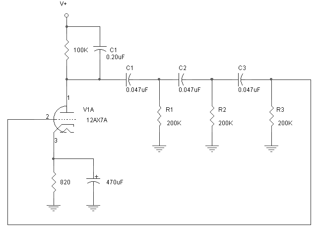
Following is a schematic diagram of a typical phase shift oscillator:
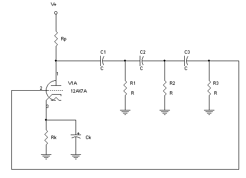
Phase Shift Oscillator
The triode is configured as an inverting amplifier to provide the necessary
gain, and the feedback network is connected from the plate to the grid.
The phase shift elements are C1/R1, C2/R2, and C3/R3. Three of these
phase lead1 networks contribute a total of 180 degrees of phase
shift at the oscillation frequency. Note that a phase shift oscillator
could also be built using four or more phase shift elements, with each element
contributing less overall phase shift at the oscillation frequency.
Normally, there is no need to do this, as it takes extra components. A
minimum of three phase shift networks is required, however, because the
maximum theoretical phase shift available from any one RC network is 90
degrees, and the actual phase shift approaches this value asymptotically.
A phase shift oscillator can also be made using three phase lag networks,
which are obtained by swapping the positions of the R and C value components
in the above schematic. The lag network would require one additional
coupling cap to block the DC on the plate voltage from the grid, and one
additional resistor to provide the grid bias ground reference for V1A, so it
is not normally used.
Following is an example of both a phase lead and a phase lag network,
designed for a 45 degree phase shift at the -3dB point of f = 1/(2*Pi*R*C) =
1/(2*Pi*1Meg*.01uF) = 15.9Hz:
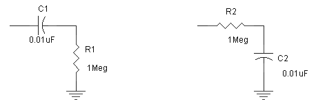
Phase Lead
Network
Phase Lag Network
Following is a plot of the phase shift and attenuation characteristics of
the phase lead and phase lag networks:
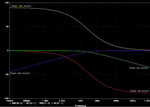
(click on image for larger view)
As can be seen from the plot, the phase lead network starts at near +90
degrees at 0.1Hz, and shifts through +45 degrees at the -3dB point of 15.9Hz,
continuing on toward 0 degrees above 1kHz. The phase lag network, on the other
hand, starts at 0 degrees, shifts through -45 degrees at the -3dB point, and
continues on towards -90 degrees above 1kHz. Either one will provide an
effective 0 degrees phase shift when three of them are combined with the 180
degree phase shift of the amplifier as shown in the phase shift oscillator
schematic.
It can be shown2 that the attenuation of the phase shift
elements in the feedback loop is 1/29, so the oscillator will oscillate if the
amplifier gain is greater than 29 (which will bring the overall loop
gain above unity gain, and satisfy the gain criterion for oscillation).
The oscillations will occur at a frequency given by the following equation:
fo = 1/(2*Pi*Sqrt(6)*R*C)
In order to obtain the lowest distortion for the best sine wave, the
amplifier should be operated with a gain of exactly 29, which is just the bare
minimum necessary to sustain oscillation. This will produce the purest
sine wave, however, it is impractical if tubes of varying gains may be
substituted (this usually requires an adjustment control to trim the gain), or
if the frequency of oscillation must be adjusted in such a manner as to change
the gain of the network. For these reasons, the gain is usually made
higher, and post-filtering of the waveform is done to remove unwanted harmonic
distortion.
If four phase lead networks are used, the phase shift per section at the
oscillation frequency is lower, therefore, the attenuation of the network is
also lower, around 1/18. This allows use of lower gain tubes if
necessary, since the gain of the amplifier only has to be at least 18.
The only way to get an oscillator like this to start
rapidly and reliably is to introduce an outside interference, in the way of a
voltage or current transient. In general, the larger the transient, the
quicker the start. The typical method of turning the tremolo on and off
is to use a footswitch that kills the biasing of the amplifier section of the
oscillator.
One of the problems with this kind of footswitch
circuit is that the amplifier is cut off by removing the bias on the cathode
with the shorting switch. In order to oscillate, it has to first amplify. The
footswitch provides the shock start in the form of a transient as the cathode
voltage rises from the short to the 1.6V nominal stable point, but the bypass
cap, which must be there in order to attain enough gain to oscillate, now
works against things by slowing down and limiting the magnitude of the startup
transient. As can be seen, the previously mentioned requirement for a
large value bypass capacitor in order to get enough gain at low frequencies is
now at odds with the requirement for a fast transient to start the oscillator
reliably. In these cases, the capacitor needs to be designed for a value
just above that required for reliable oscillation. In some cases, the
oscillator will still be slow to start, or may not start at all.
It is usually easier to get these type oscillators to
start if the amplifier stays on, biased to the proper point of operation, and
an outside AC transient is introduced somewhere in the circuit. However, this
is not so easy to do when all you have is a footswitch that must be grounded
on one side, and have a safe voltage on the other terminal, and no circuit to
generate a startup pulse to inject into the circuit.
One way to accomplish this is to add a large value
resistor from the "center resistor", or R2 as shown in the above
examples, to the power supply, and connect the footswitch to the junction of
the two resistors. Typically the resistor should be around ten times the
value of the center resistor. When the switch is grounded, the oscillator is
off, because the AC feedback path is broken, but the DC bias on the tube
remains the same, because the coupling caps on either side block the DC
voltage. This leaves the amplifier biased properly for normal operation.
When the switch is opened, there is a fast, relatively high voltage AC
transient that is coupled into the grid circuit, which starts the oscillations
rapidly. The drawback is that the junction of the two resistors is at about
1/11 the supply voltage normal operation, which means this voltage appears on
the center terminal of the footswitch, which may not be safe, particularly if
the center to ground resistor fails. Also, this circuit may not speed up the
initial power-on startup delay, only the footswitch startup delay, but this is
usually acceptable.
Appendix A: The math behind the phase shift
oscillator:
1Phase lead network analysis:
A single-section, phase lead network transfer function can be derived using
the voltage divider rule as follows:
Vo = Vi*R/(R+1/sC) = Vi*sRC/(sRC+1)
Therefore, the transfer function, H(s), is equal to:
H(s) = Vo/Vi = sRC/(sRC+1)
where s = jw = j*2*Pi*f
and j = sqrt(-1)
A complex number of the form C = A + jB has both a magnitude and a
phase. The magnitude is equal to the square root of the sum of the
squares of the real and imaginary parts, and the phase is equal to the
arctangent of the imaginary part divided by the real part, as shown below:
Magnitude H(s) = sqrt(A2 + B2)
Phase H(s) = tan-1(B/A)
Therefore, the magnitude of the phase lead transfer function is as follows:
|H(jw)| = sqrt[(wRC)2]/(sqrt(12 + (wRC)2))
= (wRC)/sqrt(1+ w2R2C2)
And the phase of the phase lead transfer function is:
ø = (phase of numerator - phase of denominator) = tan-1(wRC/0)
- tan-1( wRC/1) = 90o - tan-1( wRC)
Using the example given, R = 1Meg and C = 0.01uF:
|H(jw)| = (2*Pi*f)*(1e6)(0.01e-6)/sqrt(1 + (2*Pi*f)2*(1e6)2*(0.01e-6)2)
= (0.06283*f)/sqrt(1 + .00395*f2)
ø = 90 - tan-1(2*Pi*f*R*C) = 90 - tan-1(2*Pi*f*(1e6)(0.01e-6))
= 90 - tan-1(.06283*f)
Therefore, at a frequency of 15.9Hz, the magnitude and phase would be:
|H(jw)| = (0.06283*15.9)/sqrt(1 + .00395*15.92) = 0.707 =
-3.01dB
ø = 90 - tan-1(.06283*15.9) = 45o
If f = 0 is substituted into the equations, the resultant magnitude goes to
zero (as it should, since the capacitor blocks DC) and the resultant phase
goes to 90 degrees.
If f = infinity is substituted into the equations, the resultant magnitude
goes to 1, or 0dB, and the resultant phase shift goes to zero.
A plot of the magnitude and phase of the transfer function can be made by
substituting in values of f and solving for the resulting magnitude and
phase numbers.
It is important to note that the frequency at which a 60 degree phase
shift occurs in a single phase lead section is not the same frequency at
which a 180 degree phase shift occurs in a three section phase lead network,
so you can't just solve the single-section phase equation for frequency, and
plug in a value of 60 degrees to find the resultant frequency at which
oscillation will occur for given values of R and C. The procedure for
determining frequency of oscillation for a three-section phase lead network
is described in the next section on phase shift network analysis.
2Phase shift network analysis:
The transfer function of the phase shift network can be determined as
follows:
Using mesh analysis, and substituting general impedance variables Z1
for C and Z2 for R, the following three equations can be derived:
(1) Vi = Z1I1 + Z2(I1-I2)
(2) 0 = Z2(I2-I1) + Z1I2
+ Z2(I2-I3)
(3) 0 = Z2(I3-I2) + Z1I3
+ Z2I3
This can be rearranged and written in terms of the mesh currents as follows:
(1) Vi = (Z1+ Z2)I1 - Z2I2
(2) 0 = -Z2I1 + (Z1+2Z2)I2
- Z2I3
(3) 0 = -Z2I2 + (Z1+ 2Z2)I3
which gives the following matrix equation:
[Vi] [I1]
[(Z1+ Z2) - Z2
0 ]
[0] = [I2] [ -Z2
(Z1+ 2Z2) - Z2
]
[0] [I3]
[
0 -Z2
(Z1+2Z2) ]
This matrix can be solved for the individual currents by using Cramer's
Method as follows:
First, the characteristic determinant of the matrix is calculated as
follows:
| (Z1+
Z2) - Z2
0 |
Det = | -Z2 (Z1+
2Z2) - Z2
| = Z13 + 5Z12Z2+
6Z1Z2 2 + Z2 3
|
0 -Z2
(Z1+2Z2) |
Next, the individual currents can be solved by substituting the voltage
matrix into the appropriate position in the numerator matrix and solving the
resulting determinant, and dividing by the characteristic determinant as
follows:
| (Z1+
Z2) - Z2
Vi
|
Z22
I3 = | -Z2
(Z1+ 2Z2)
0 |
= Vi *
____________________
|
0 -Z2
0
|
Z13 + 5Z12Z2+ 6Z1Z22
+ Z2 3
_________________________
Z13 + 5Z12Z2+ 6Z1Z22
+ Z2 3
I3 was chosen first so the output voltage could be determined in
order to derive the transfer function. Since I3 is now
known, the output voltage is simply I3 multiplied by the last
shunt impedance, Z2 :
Z2 2
Vo = Vi *
_________________________ *Z2
Z13 + 5Z12Z2+ 6Z1Z22
+ Z2 3
Z23
= Vi
* _________________________
Z13 + 5Z12Z2+ 6Z1Z22
+ Z2 3
Therefore, the transfer function is:
Z23
Vo/Vi =
_________________________
Z13 + 5Z12Z2+ 6Z1Z22
+ Z2 3
This can be rewritten by dividing the numerator and denominator by Z23
as follows:
1
Vo/Vi =
_________________________
Z13/Z23 + 5Z12/Z22+
6Z1/Z2 + 1
Now, substituting the variable 'x' for Z1/Z2,
1
Vo/Vi =
_________________________
x3 + 5x2 + 6x + 1
The criteria for oscillation is positive feedback, i.e., the total phase
shift around the loop have to be equivalently zero (a multiple of 360
degrees) and a gain of unity or greater. This criterion can be met by a
total phase shift through the network of 180 degrees, since the amplifier
contributes 180 degrees to the phase shift through it's inversion. In
order for the phase shift to be 180 degrees, the imaginary parts of the
transfer function must be zero. The squared term, 5x2 and
the constant 1, are purely real, since the square of j is equal to -1, so
the following equation must be met for a zero imaginary part:
x3 + 6x = 0
which gives:
x2 = -6
so:
x = + sqrt(-6) = + j*sqrt(6)
If x3 + 6x = 0, the magnitude equation at the frequency of
oscillation simplifies to:
1
Vo/Vi =
__________
5x2 + 1
Substituting x = - j*sqrt(6) into this equation for x (-j because Z1
is a capacitor) gives:
1
1
Vo/Vi =
__________
= __________
= - 1/29
5(- j*sqrt(6))2 +
1
5*(-1*6)+1
This means that the transfer function of the phase shift network has a
gain of 1/29, and the negative sign indicates a phase inversion of 180
degrees. Therefore, in order to satisfy the gain criterion for
oscillation, the amplifier must have a gain of -29 (once again, the negative
sign indicating phase inversion of 180 degrees). The gain can be higher than
this, but the distortion will be lowest at the minimum gain necessary to
sustain oscillations.
The frequency of oscillation is also determined by the above oscillation
criteria, as shown below:
Since x = Z1/Z2 = (1/(jwC))/R = 1/(jwRC) =
-j*sqrt(6),
w = 1/(sqrt(6)*R*C)
Since w = 2*Pi*f,
f = 1/(2*Pi*sqrt(6)*R*C)
This is the frequency which will give a total phase shift through the
network of -180 degrees, which will result in oscillation.
The input impedance of the network can be determined by first calculating
I1 with a Vi of 1V, then taking the reciprocal of it. This
is done as follows:
|
1 - Z2
0
|
Z12 + 4Z1Z2+ 3Z22
I1 = |
0 (Z1+ 2Z2)
-Z2
| =
____________________
|
0 -Z2
(Z1+ 2Z2)
|
Z13 + 5Z12Z2+ 6Z1Z22
+ Z2 3
_________________________
Z13 + 5Z12Z2+ 6Z1Z22
+ Z2 3
Taking the reciprocal to get the input impedance gives:
Z13 + 5Z12Z2+ 6Z1Z22
+ Z2 3
Zin =
____________________
Z12 + 4Z1Z2+ 3Z22
Dividing both numerator and denominator by Z23, after
multiplying the denominator and the entire equation by Z2/Z2,
(to make the function proper in terms of degree of exponents in the
numerator and denominator) gives:
Z13/Z23+ 5Z12Z2/Z23+
6Z1Z22/Z23 + Z23/Z23
Zin = Z2
* _________________________________
Z12Z2/Z23 + 4Z1Z22/Z23+
3Z23/Z23
This simplifies to:
Z13/Z23+ 5Z12/Z22+
6Z1/Z2+ 1
Zin = Z2
* ___________________________
Z12/Z22 + 4Z1/Z2+
3
Substituting the variable 'x' for Z1/Z2,
x3 + 5x2 + 6x + 1
Zin = Z2 *
_______________
x2 + 4x + 3
At the frequency of oscillation, Zin becomes:
(- j*sqrt(6))3 + 5(-j*sqrt(6))2 + 6(-j*sqrt(6)) + 1
Zin = Z2 *
_______________________________________
(- j*sqrt(6))2 + 4(- j*sqrt(6)) + 3
Simplified, this becomes:
- 29 Z2
- 29 Z2
Z2
Zin = ______________ =
______________ = ______________
-3 -
4j*sqrt(6)
-3 -
j9.798
0.103 + j0.338
This impedance equation indicates that the input impedance at the
oscillation frequency is proportional to Z2, but not Z1.
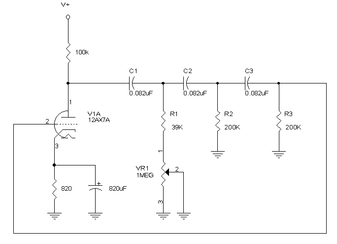
If the frequency is to be varied, this impedance must remain constant, or
the amplitude of the oscillations will vary. If the gain of the
amplifier is set to the critical value of 29, and the impedance decreases,
the gain will drop and the oscillations will decay to zero. Likewise, if the
impedance increases, the gain will increase, and the oscillation amplitude
will increase, and there will also be an increase in the distortion in the
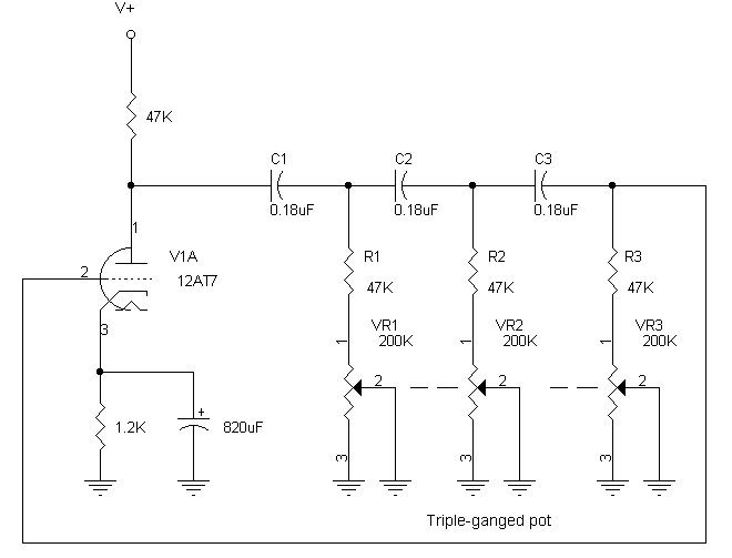
output. Therefore, the best method of varying the frequency of
oscillation is to vary all three Z1 impedances
simultaneously. This will require a triple-gang variable capacitor,
which is not practical at the low frequencies involved in audio oscillators
used in tremolo circuits. A better approach would be to use the phase
lag network version, and vary the three Z1 impedances
simultaneously with a triple-gain potentiometer, since they are resistances
in the phase lag configuration. This requires an extra isolation
capacitor as well as an extra bias resistor, which must be large in relation
to the series resistance, to avoid loading the network. In addition,
the phase lag version has much higher distortion of the sine wave at the
plate output. Alternately, the gain of the amplifier could be made
much larger than 29, and the output will have amplitude variations as well
as distortion of the sine wave as the amplitude is adjusted. The
amplitude variation is not too much of an issue with a guitar amplifier,
because it is normal to set the speed and then adjust the intensity to the
desired level. Also, the amplitude variations can be minimized by
making the phase shift network impedance much larger than the output
impedance of the amplifier stage.
Copyright © 1999,
2000 Randall Aiken. May not be reproduced in any form without written
approval from Aiken Amplification.