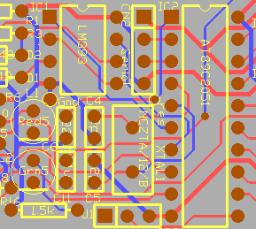
The Printed Circuit Board Layout
The Printed Circuit Board (PCB) is the laminate to which all the electronic components are soldered, with one or more layers of etched metal tracks making the connections. The components and connections in the PCB Layout are derived from the circuit diagram, and physically placed and routed by the designer to get the best result. The PCB Layout defines the final physical form of the circuit, and enclosure and labeling details can be finalized as the layout is completed.
When the PCB layout is complete, the final CAD file is sent (by modem or internet) to a subcontract PCB laminate manufacturer. The manufacturer returns the etched PCB laminates a few days later, ready for assembly into prototypes. In certain companies, manufacturing of the laminate is not done as designing is the area of expertise. Manufacture of laminates requires raw materials and more machinery, thus increase in manpower. This hampers the designing process itself as expertise and concentration is needed for the laminate production as well. Hence the solution is to hire the services of the subcontract PCB laminate manufacturer.
The Printed Circuit Board (PCB) Layout --- Detail: The design process
The connections on the PCB should be identical to the circuit diagram, but while the circuit diagram is arranged to be readable, the PCB layout is arranged to be functional, so there is rarely any visible correlation between the circuit and the layout.
PCB layout can be performed manually using CAD software or in combination with an Autorouter. The old method of PCB layout is by drawing or using stick on paper shapes on Mylar film. But this method is time consuming and decreases productivity.
The CAD PCB layout consists of several layers, for illustration purposes the holes, outline and component identification layers are usually combined into one diagram.
Currently, due to the high demand from customers, most of our PCB’s have the following characteristics:
1.Double sided Laminate- economical and space saving for complex circuitry.
2.Two layers of copper tracks, one each side of the board.
3.Plated Through Hole (PTH) - each hole is copper plated providing a circuit between the sides of the PCB.
4. Fibreglass-resin laminate (FR4)
5.Solder Mask Over Bare Copper (SMOBC) - green insulating ink everywhere except connections.
6.Component legend -Identifying lettering, component outlines and values in white or yellow ink
7.Tinned -Tinning is application of Solder to all exposed copper, increasing solder ability.
8.Hot oil leveled - Hot oil or hot air leveling makes the tinning flat, so that surface mount components can be positioned reliably.
PCB CONSTRUCTION.
PCB construction methods have undergone several advancements recently, due to improved technology. Obviously research plays an important part of engineering, even for PCB design and layout.
Different methods of PCB construction:
1.Conventional
A rigid PCB of thickness 1.6mm, with wire-leaded components mounted on only one side of the PCB, with all the leads through holes, soldered and clipped. Conventional circuitry is generally easier to debug and repair than Surface mount.
2.Surface Mount Technology (SMT) or devices (SMD)
A PCB with tag-leaded components soldered flush to PCB pads. Holes are still needed on the PCB, but not where the component leads are attached. Surface mount circuitry is generally smaller than conventional. Surface mount is generally more suited to automated assembly than conventional.
3.Surface mount & conventional mix
In practice, most boards are a mix of surface mount and conventional components. This can have its disadvantages as the two technologies require different methods of insertion and soldering.
4.Double sided Laminate
A bare PCB laminate having tracks on both sides, normally with PTH holes connecting circuitry on the two sides together.
5.Double sided Component Assembly
Mounting components on both sides of the PCB. Normally only surface mount circuitry would be mounted on both sides of a PCB.
6.Multi-layer
A PCB Laminate may be manufactured with more than two layers of copper tracks by using a sandwich construction. The cost of the laminate reflects the number of layers. The extra layers may be used to route more complicated circuitry, and/or distribute the power supply more effectively.
7.Gold plated
Certain areas on a PCB may be gold plated for use as contact pads. Unless the whole PCB is gold plated before etching, this technique is limited in its application, normally, to pads on the edge of a PCB, as an electrolytic plating bar must be attached to the pads, and then removed part way through the PCB manufacturing process.
8.Flexible PCB
A technique used extensively with membrane keyboards, combination connector/circuit boards, and circuit boards to fit in awkward shapes - eg cameras.
9.Chip On Board (COB)
Where the IC die is attached direct to a PCB, and bond out wires from the IC connect directly to PCB lands. The chip is then covered with a black blob of epoxy. A technique used mostly with very high volume, cost sensitive applications, eg musical greeting cards.
10.Phenolic PCB
As distinct from Fibreglass, Phenolic is a cheaper PCB laminate material.
11.Daughterboard
A circuit board mounted to another circuit board - such as a plug in card.
An Introduction l The Specifications l EMI-Firmware l EMI-Pilot Run l EMI - The Circuit Design l Back To Index Equipment and Machinery used for PCB Manufacture l Printed Circuit Board Etching l Design Methods